
Characteristics of Grinding Wheels for Mass Production Back Grinding
As semiconductor devices continue to advance toward higher integration,smaller form factors, and improved performance, the requirements for wafer thinning and high-quality surface finish have become increasingly stringent.
Wafer back grinding is a critical process in the semiconductor back-end manufacturing flow. Its primary purpose is to thin the backside of the wafer to the required thickness while reducing total thickness variation (TTV),controlling warp/bow, and maintaining both surface roughness and wafer strength to meet the needs of subsequent dicing, packaging, and assembly processes.
Under mass production conditions, back grinding wheels must not only provide strong material removal capability, but also balance processing efficiency, wheel life, process stability, and wafer quality. In particular, when processing different wafer materials such as Si, SiC, and GaN, differences in hardness, brittleness, thermal conductivity, and machinability directly affect grinding performance. As a result, the abrasive type, grit size, concentration, bond system, and pore structure of the grinding wheel all have a direct impact on its performance.
Therefore, grinding wheels used in mass production back grinding are not designed simply to maximize cutting speed. Instead, they must achieve an optimal balance among material removal rate, grinding load, self-sharpening ability, surface quality, and service life. Selecting the appropriate wheel characteristics according to wafer material and equipment conditions, and establishing stable and repeatable production parameters, has become a key factor in improving both efficiency and yield in wafer thinning processes.
Example: The following illustrates the current behavior observed during continuous grinding of three wafers on a DISCO grinder in Japan. The machine’s maximum current setting is 20A, while the safe continuous processing current is kept below 16A to reduce the risk of wafer breakage, especially when thinning below 100 μm, and to limit residual stress in the wafer, thereby reducing warp.
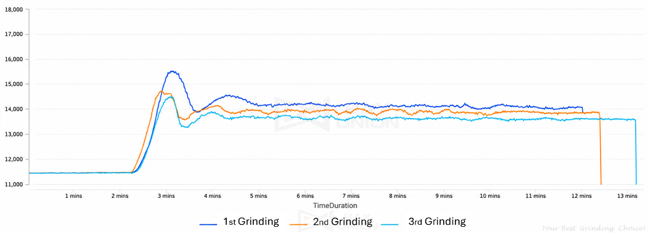
With a well-designed grinding wheel, the current profile during continuous grinding of three wafers shows the following:
1. The current at the moment the wheel first contacts the wafer is maintained at 14.5A to 15.5A, staying within the customer’s specified range.
2. The difference between the peak contact current and the current during grinding remains within 2A, indicating a relatively small instantaneous load variation on the wheel and a reduced risk of wafer breakage.
3. During approximately 8 minutes of continuous grinding, the wheel maintains good self-sharpening performance, and the current remains stable until completion.
To meet different customer requirements for back-side wafer thinning, Bay Union can provide multiple grinding wheel formulations that satisfy mass production requirements while moderately reducing dependence on imported consumables. For further information, please contact Bay Union Sales at , and we will arrange a professional team to assist you promptly.